The Brightest Solutions for Bright Messages

SMART DISPLAY SOLUTIONS
Genoptic, utilizing advanced nano-technologies, has integrated its advanced Smart IC Power Chip solution to combine; power circuitry, RF communication, and control system into a single integrated circuit microchip. The advanced chip fully eliminates the need for LED drivers and MOSFETs, for dimming purposes, due to its multi-output structure, which independently controls each LED. This low-cost solution improves efficiency, increases power density, enhances reliability, and simplifies thermal management.
Integrated Solution for LED Sign Applications
Genoptic integrates its new advanced solution, which combines various components (i.e., power circuitry, RF communication unit, and control system) into an integrated circuit microchip using advanced nano-technology.
The Genoptic LED Power IC is able to:
- Significantly improve efficiency
- Substantially increase power density
- Enhance reliability
- Simplify the thermal management of the LED Module
Genoptic’s nano-technology-based integrated circuit chip prototypes are highly compact, low cost, energy efficient, and extremely reliable. Genoptic has filed several patents on various innovations used in this proposed solution, which currently covers 14 patent families and growing.
The main advantage of the Genoptic chip architecture is that it allows for a high voltage power distribution, which significantly reduces power losses and in turn increases the overall efficiency of the LED Module. Also, the resulting high voltage power distribution better accommodates the integration of solar panels/batteries to the digital LED signage displays.
The Advanced LED Power IC fully eliminates the need for LED drivers and MOSFETs, for dimming purposes, due to its multi-output structure, which independently controls each LED.
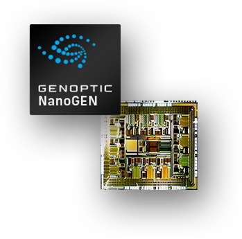
Genoptic’s new LED driver IC uses a novel high-efficiency, constant-current architecture. The first prototype of the IC was fabricated using 0.35 µm CMOS technology. A die micrograph of the prototype is shown in Fig. 1. The dimensions of the silicon die are 4.03 mm x 2.69 mm (10.8 mm2) with further optimizations in size expected to reduce the total silicon area to less than 2.5 mm x 2.5 mm for future design iterations.
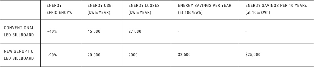
Typical digital LED billboards are comprised of tens of thousands of LEDs which are running continuously. Over a year, a typical LED billboard uses tens of thousands of kWh in energy, which is substantially more than an average home. Enormous amounts of energy are being wasted by digital LED billboards that use conventional LED driver solutions. Thus incurring significant financial and environmental costs.
A case study comparing the energy consumption of a typical LED billboard using the conventional driver architecture and Genoptic’s new high-efficiency driver is summarized in Table I. The LED sign powered by Genoptic’s driver IC is expected to consume ~55% less energy and save approximately $25,000 in energy costs over the course of the LED billboard’s lifespan (i.e. 10 years).
Energy savings of conventional vs Genoptic LED billboard